
Huawei’s EUV breakthrough
China’s EUV breakthrough: Huawei, SMIC reportedly advancing LDP lithography, eye 3Q25 trial, 2026 rollout
“LDP is much more efficient than LPP, which ASML uses,” Dr Kim
SMT&Packaging • March 11, 2025 ~ TomHardware AsiaTimes
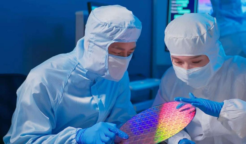
China is advancing in extreme ultraviolet (EUV) lithography, with a domestically developed system undergoing testing at Huawei’s Dongguan facility, according to XFastest and Wccftech. Trial production is reportedly set for the third quarter of 2025, with mass production targeted for 2026, according to a recent report in DigiTimes Asia.
The system employs laser-induced discharge plasma (LDP) technology, a non-ASML alternative to laser-produced plasma (LPP), positioning China as a potential challenger to ASML’s dominance in EUV lithography.
LDP vs LPP: a technological comparison
China’s LDP-based EUV system produces 13.5nm EUV light by evaporating tin between electrodes and then ionizing it through high-voltage discharge, creating a plasma source for lithography.
Unlike ASML’s LPP method, which depends on high-powered lasers and FPGA-driven real-time controls, LDP offers a different approach to achieving EUV light generation. The key differences include:
LPP (ASML’s technology):
● Relies on high-power lasers to generate EUV plasma
● Proven and stable for high-end semiconductor manufacturing
● Industry-standard technology for advanced chip production
● Expensive and technically demanding
LDP (China’s alternative):
● Uses laser and electrical discharge for EUV generation
● Lower-cost alternative with local supply chain control
● Still in development, with challenges in power output and stability
Dr Kim, a TSMC researcher and former Samsung and IBM expert, stated on X:
“China is out-competing ASML. The LDP EUV generation commercialization push is a DeepSeek moment for lithography that I was fearful of.
“LDP is much more efficient than LPP, which ASML uses.”
Tech entrepreneur Jude Gomila, followed by OpenAI CEO Sam Altman, reshared Kim’s post, amplifying industry attention on China’s EUV progress.
Kim also quoted Yin Sun on X, who stated:
“China’s domestically developed EUV machine, utilizing LDP technology—distinct from the LPP approach employed by ASML—is currently undergoing testing at Huawei’s Dongguan facility. Trial production is slated for the third quarter of 2025, mass production for 2026.”
“It’s over.” Kim’s response.
A potential shift in the semiconductor landscape
Due to US export restrictions, China has been unable to obtain ASML’s EUV machines, forcing domestic chipmakers to rely on deep ultraviolet (DUV) lithography, which operates at 248nm (KrF) and 193nm (ArF) wavelengths.
Although 193nm immersion lithography is the most advanced pre-EUV solution, it still requires multi-patterning to produce leading-edge semiconductor nodes.
If China commercializes LDP-based EUV lithography by 2025-2026, could it bypass Western technological restrictions? The answer: Possible, but significant hurdles remain.
Key considerations for China’s EUV breakthrough
1. Achieving technological autonomy
● ASML’s EUV systems rely on a global supply chain, including Cymer lasers (US), Zeiss optics (Germany), and Dutch engineering.
● Mass production of LDP-based EUV machines could allow China to lessen its reliance on ASML and Western semiconductor suppliers.
2. Overcoming power and manufacturing hurdles
● LDP prototypes currently produce 50-100W, but at least 250W is required for commercial-scale EUV lithography.
● Key manufacturing challenges include multilayer mirrors (MLMs), photomasks, and photoresists, which remain bottlenecks.
● China’s Changchun Institute of Optics is developing optical components, but Zeiss maintains a significant lead in precision optics.
3. Huawei & SMIC’s role in adoption
● SMIC, China’s top foundry, is working with Huawei to incorporate LDP-based EUV scanners into its chip production process.
● Scaling China’s semiconductor ecosystem will take years, as EUV technology must be validated at commercial volumes.
● If SMIC successfully integrates LDP-based EUV, it could close the gap with TSMC and Samsung in advanced node manufacturing.
4. Market competition & geopolitical impact
● If China successfully scales EUV production, it will become the only nation outside the Netherlands to achieve EUV lithography capabilities.
● Initial production capacity will likely be constrained, giving ASML and TSMC time to sustain their lead.
● The US and allied nations may impose further export controls on photoresists, mask blanks, and critical semiconductor materials to curb China’s progress.
5. The long-term roadmap
● Third-quarter 2025 trial production would confirm China’s ability to generate stable EUV power at scale.
● 2026 mass production could signal China’s entry into 5nm semiconductor manufacturing.
● If LDP-based EUV advances further, China may pursue 3nm or even 2nm nodes by 2030.
Conclusion: a potentially disruptive development
If China commercializes LDP-based EUV lithography, it could represent a major technological shift, cutting reliance on ASML and altering the global semiconductor landscape. However, challenges remain in scaling production, enhancing power output, and navigating Western trade restrictions.
By 2030, if China establishes an independent EUV supply chain and achieves 3nm or 2nm chip production, it could challenge ASML, TSMC and Samsung in advanced semiconductor manufacturing.
China’s Harbin Institute of Technology has successfully developed an EUV light source based on discharge plasma, producing 13.5nm radiation. Once dismissed as speculation, this breakthrough suggests that China’s semiconductor advancements may be underestimated by Western analysts.
The next few years will determine whether China’s EUV ambitions translate into reality or remain a long-term objective constrained by geopolitical and technical barriers.
For more, see China leads US in semiconductor research

